· Nacho Planas
The AI supply chain adventure: How minerals become LLMs
Every answer a chatbot gives you has passed through a quartz mine, a Dutch light source, a Taiwanese packaging line, a Korean memory stack, a copper spine, a gas turbine and a training run that cost more than most companies are worth. Here is the whole chain, thirteen layers deep, with the companies that hold each one and what makes them hard to replace.
Disclaimer: Not investment advice. This is an essay about how an industry fits together. Figures are as reported by companies, governments and research firms up to 26 September 2026. Where a number is an analyst estimate, I say so.
One answer, thirteen industries
Ask a chatbot a question and the answer seems to come from nowhere. It actually comes from one of the longest supply chains humans have built. Before those words reached your screen, someone mined quartz in North Carolina and copper in Chile, a German chemical company purified silicon to eleven nines, a Dutch machine fired fifty thousand droplets of molten tin a second, a Taiwanese fab stacked two dies and eight memory towers onto one package, a Korean company thinned DRAM to the width of a hair and piled it twelve high, and a Texas data centre burned natural gas to feed a rack that weighs as much as a car and draws as much power as a hundred homes.
Then a model trained over months on tens of trillions of words read your prompt in a fraction of a second and wrote the answer one token at a time.
This essay follows that journey from start to finish: how a handful of minerals becomes a large language model. That means every layer from the ground up, what physically happens in each, which companies hold it, and what makes each of them hard to replace. It's long, because the trip is long. The map comes first.
A few things are worth knowing before we start.
- The chain isn't a line, it's a funnel. Thousands of suppliers at the bottom narrow to a handful of chokepoints in the middle (one company makes the lithography machines, one foundry makes almost every accelerator, three companies make all the high-bandwidth memory) and then widen again into thousands of buildings and millions of apps.
- The binding constraint keeps moving. In 2023 it was packaging, in 2024 memory, in 2025 electricity and turbines, in 2026 memory again, plus lasers and CPUs. Whoever holds the current bottleneck has pricing power for a while.
- Everything is growing, but not at the same speed. I've put the growth rates of every layer side by side at the end.
Layer 1: the ground
Silicon starts as quartz, and purity is measured in nines
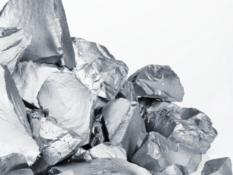
Silicon is the second most common element in the Earth's crust, so its scarcity isn't in the atoms. It's in the purity.
The journey starts with quartz (silicon dioxide) and carbon in an electric arc furnace, which produces metallurgical-grade silicon at about 99% purity. China made 4 million tonnes of it in 2025, close to 80% of the world's supply, according to the US Geological Survey. Most of it goes into aluminium alloys and silicones. By one US government estimate only about 12% becomes polysilicon, and almost all of that goes into solar panels.
The polysilicon that chips are grown from is different in kind. It has to be at least eleven nines pure: 99.999999999%, about one stray atom per hundred billion. Solar-grade polysilicon runs between six and ten nines. According to the Semiconductor Industry Association's 2025 filing to the US Commerce Department (using TECHCET data), semiconductor-grade material is just 2.4% of world polysilicon demand, about 33,500 tonnes against 1.38 million tonnes of solar grade. It can cost up to thirty times more to make. China has 94.7% of the world's polysilicon capacity, but almost all of it is solar grade; the SIA says China lacks the equipment and know-how to make the chip grade at scale.
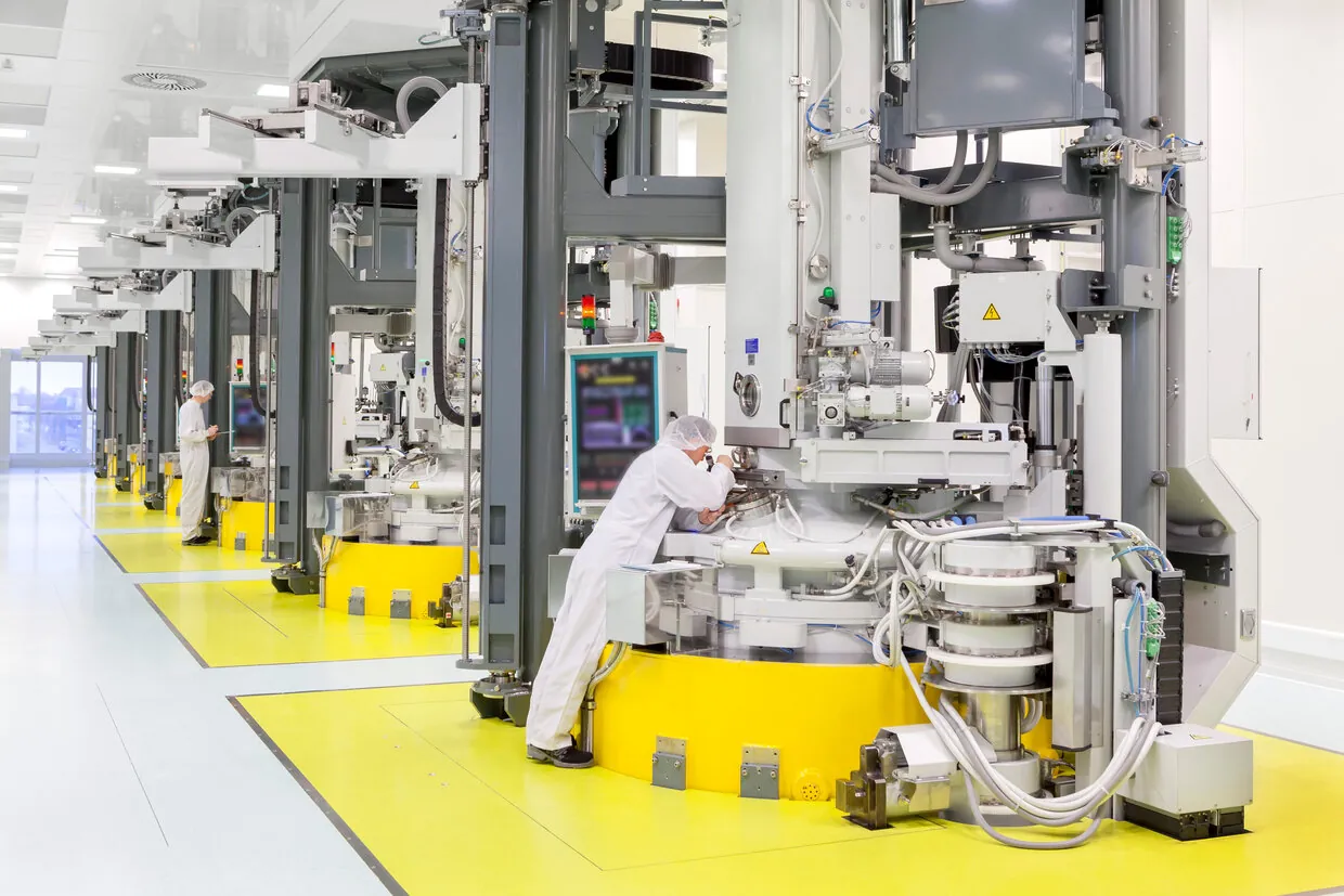
Two companies, Wacker Chemie in Germany and Hemlock Semiconductor in Michigan, supply about three-quarters of chip-grade polysilicon. Tokuyama, SUMCO and OCI make most of the rest. The polysilicon is melted and a seed crystal is slowly pulled out of the melt (the Czochralski method), growing a single crystal ingot about seven feet long and weighing about 600 pounds. It's sliced into 300 mm wafers, polished flatter than almost anything else humans make, and shipped to fabs.
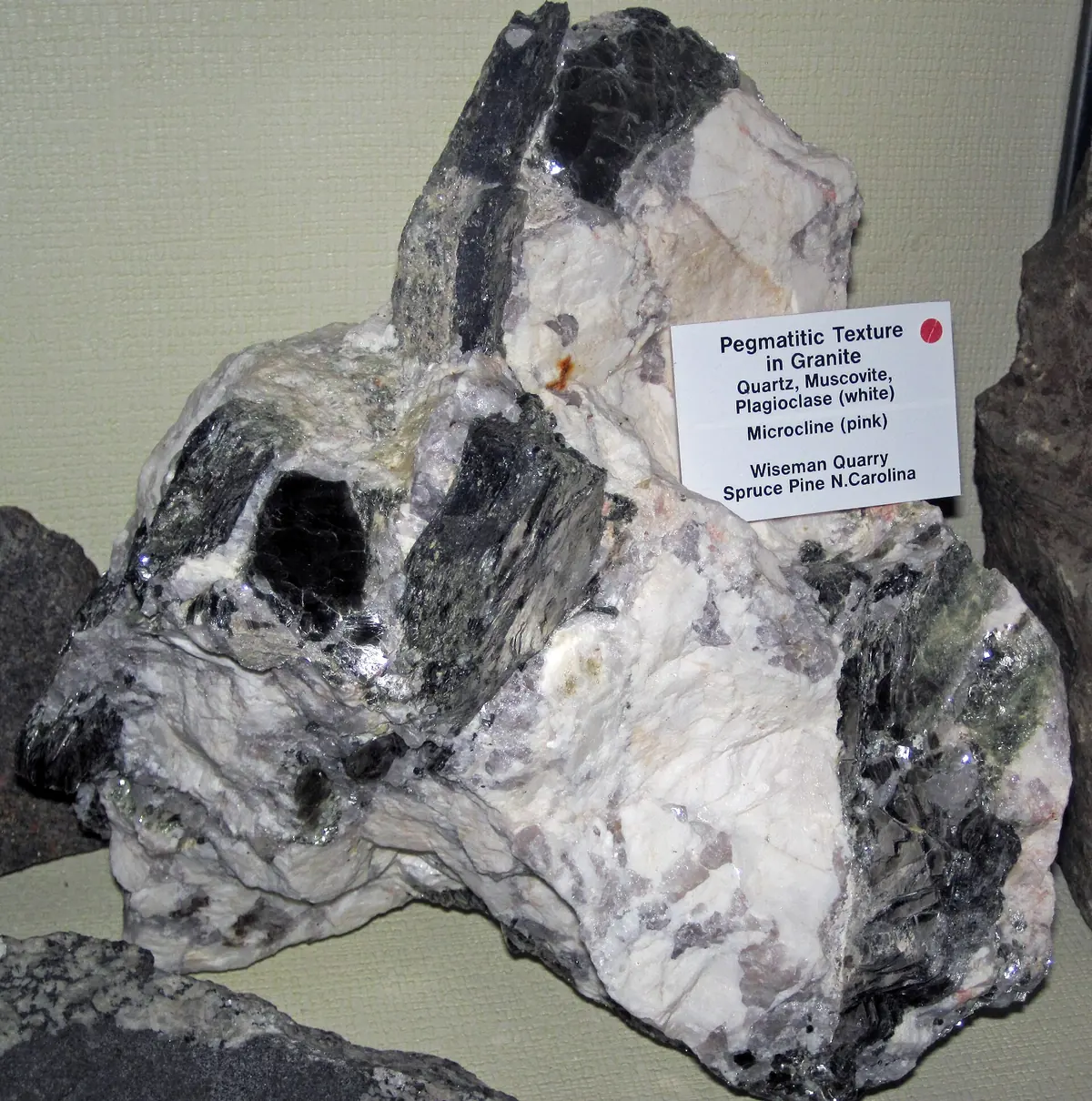
The melt sits in a crucible made of quartz, and this is where a small town in the Blue Ridge Mountains matters. Spruce Pine, North Carolina, has unusually pure quartz deposits, mined by Sibelco and The Quartz Corp, which the industry has relied on for crucibles for decades. When Hurricane Helene flooded the area in September 2024, both operations stopped. Sibelco restarted on 10 October and ramped back up. The damage turned out to be manageable, but for two weeks the world learned how much depended on one valley. People often say Spruce Pine supplies 70–90% of the world's ultra-high-purity quartz. I haven't found a primary source for that number, but nobody disputes that it's the main one.
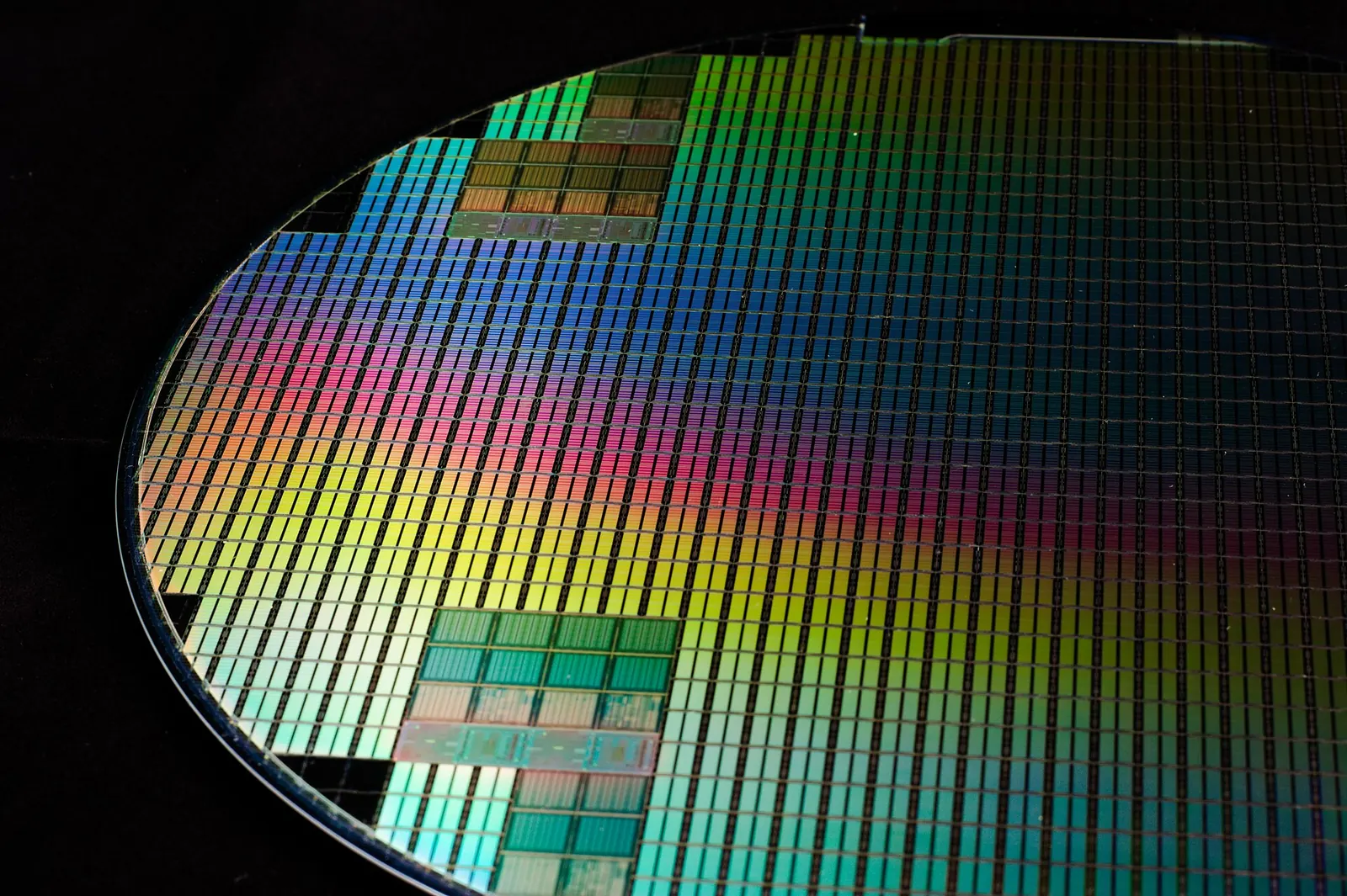
Wafers are their own concentrated business. Shin-Etsu and SUMCO, both Japanese, supply roughly half of the world's 300 mm wafers by market-research estimates; GlobalWafers (Taiwan), Siltronic (Germany) and SK Siltron (Korea) make most of the rest. SEMI counts 12,973 million square inches shipped in 2025, up 5.8%, with AI demand for logic and HBM wafers doing the lifting.
A useful number for later: one 300 mm wafer yields roughly 60 candidates for a GPU die at the maximum size a lithography machine can print. After defects, perhaps 40–50 are good, and a Blackwell GPU needs two of them. So a wafer that costs around $20,000–30,000 to process at a leading-edge node becomes somewhere between twenty and thirty GPUs that sell for tens of thousands of dollars each. That's my own estimate from the standard dies-per-wafer formula, not a company number, but it explains why TSMC can charge what it does.
The minerals that aren't silicon
A chip, and the data centre it sits in, needs a long list of other elements. Gallium goes into radio-frequency chips and some lasers. Germanium goes into fibre optics and infrared optics. Indium, as indium phosphide, is the material that turns electrical signals into laser light in every optical transceiver. Tungsten forms the contacts and plugs that connect a transistor to its wiring. Fluorspar becomes the fluorine chemistry used to etch and clean wafers. Rare earths go into magnets for fans, pumps, drives and turbines. And copper goes into almost everything: busbars, cables, transformers and motors.
Across that list, China is the dominant refiner.
China produced 99% of the world's primary gallium in 2025, mined 79% of its tungsten and 82% of its natural graphite, and refines 69% of its indium. Its share of copper smelting capacity has risen from about 15% to 50%, according to the IEA's 2026 critical minerals outlook, which also found that the top three refiners' average share across key minerals rose to 86% in 2024.
China has used that position. In December 2024 it banned exports of gallium, germanium and antimony to the US. In February 2025 it added tungsten, indium and others to its licensing regime; indium phosphide wafers need a permit, which is why AXT, a US-listed supplier whose factories are in China, lists permits as a business risk even as its revenue has more than doubled. In October 2025 China announced sweeping rare-earth controls. Then came a truce. In November 2025 China suspended the gallium, germanium and antimony ban until 27 November 2026 (licences still apply), and paused the October rare-earth rules. At the Trump–Xi summit in Washington on 24–25 September 2026, the trade truce was extended for another two months, to 10 January 2027. None of this has been resolved; it's been deferred.
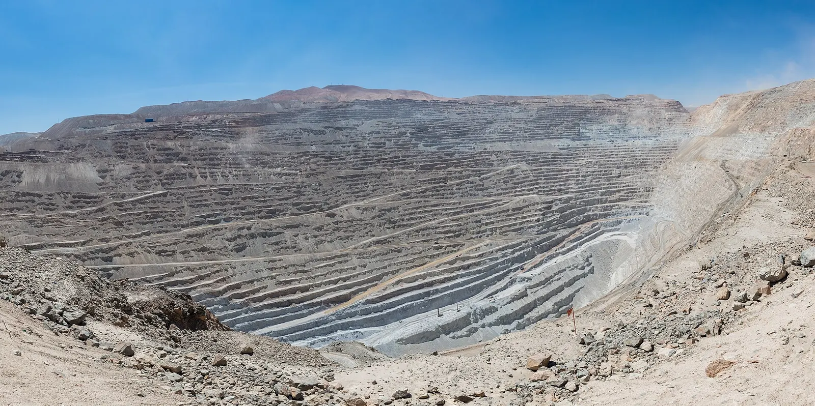
Copper deserves its own line, because AI uses it in bulk. NVIDIA's own engineers wrote in 2025 that a one-megawatt rack fed at 54 volts needs up to 200 kg of copper busbar, which comes to about 200 tonnes for a one-gigawatt site in busbars alone. That's before cables, transformers and generators. Copper hit a record of about $6.80 a pound in early September 2026 and is up about 42% on the year. The largest producers are Codelco and BHP in Chile and Freeport-McMoRan, whose Grasberg mine in Indonesia is one of the biggest in the world.
Layer 2: materials
The next stop on the trip, between the mine and the fab, is a layer of specialty materials that almost nobody outside the industry has heard of, and that the industry can't work without.
- Photoresists, the light-sensitive coatings that lithography prints onto, come mostly from Japan: JSR, Tokyo Ohka Kogyo, Shin-Etsu and Sumitomo Chemical.
- Specialty gases such as fluorine compounds, neon, tungsten hexafluoride and ultra-pure nitrogen come from industrial gas majors like Linde, Air Liquide and Nippon Sanso. Before 2022, about half of the semiconductor-grade neon came from two Ukrainian companies. The industry has since diversified.
- Ajinomoto build-up film (ABF) is the one that surprises people. Ajinomoto is the Japanese company famous for MSG. In the 1990s its chemists realised that the epoxy resins from their amino acid research could be made into a thin insulating film. Since 1999 that film has been the layer that carries the fine wiring inside nearly every high-performance chip package. Ajinomoto's share is commonly put above 95%; the company won't give a figure, but no serious competitor exists.
- Glass cloth made from special low-expansion "T-glass" is the stiff core inside those package substrates. Nittobo, a Japanese textile company, is the dominant supplier, and in 2026 Apple, NVIDIA, Google and Amazon were reported to be competing for its output.
- Substrates themselves are built by Ibiden, Unimicron, Shinko and AT&S. Intel, and SKC's Absolics, are developing glass-core substrates that could replace organic ones later in the decade.
And then there's glass of a different kind.
Corning, and the return of the fibre business
Corning invented low-loss optical fibre in 1970. For most of the next fifty years that was a steady business: telecom carriers bought fibre in cycles. AI changed the demand curve. Inside an AI data centre, thousands of GPUs have to talk to each other at once, and every one of those links beyond a few metres is light in glass. Corning says generative AI data centres need many times more fibre than traditional ones.
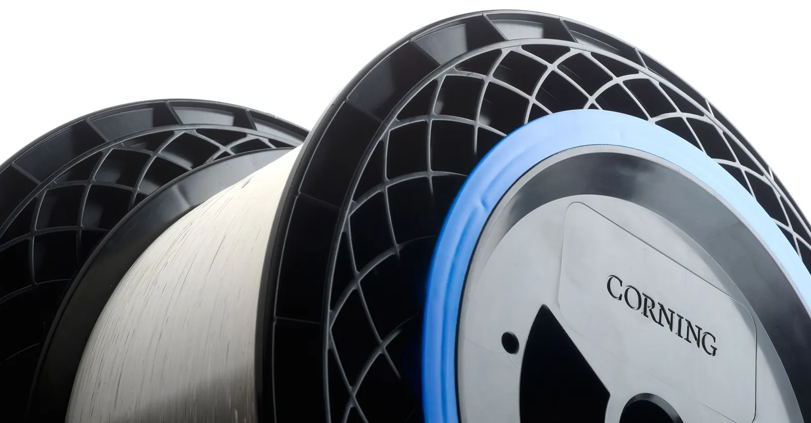
The numbers moved quickly. In its second quarter of 2026, Corning's Optical Communications sales rose 32% to $2.07 billion, and the enterprise segment, which is mostly data centres, grew 65%. Optical is now close to half of Corning's sales. In January 2026 Meta signed a multiyear deal worth up to $6 billion for fibre, cable and connectivity, anchoring an expansion of Corning's cable plant in Hickory, North Carolina. Amazon signed a multibillion-dollar deal too, and NVIDIA announced a partnership aimed at expanding US optical connectivity capacity tenfold. Corning's "Springboard" plan targets a $20 billion annual sales run-rate by the end of 2026 and $40 billion by 2030.
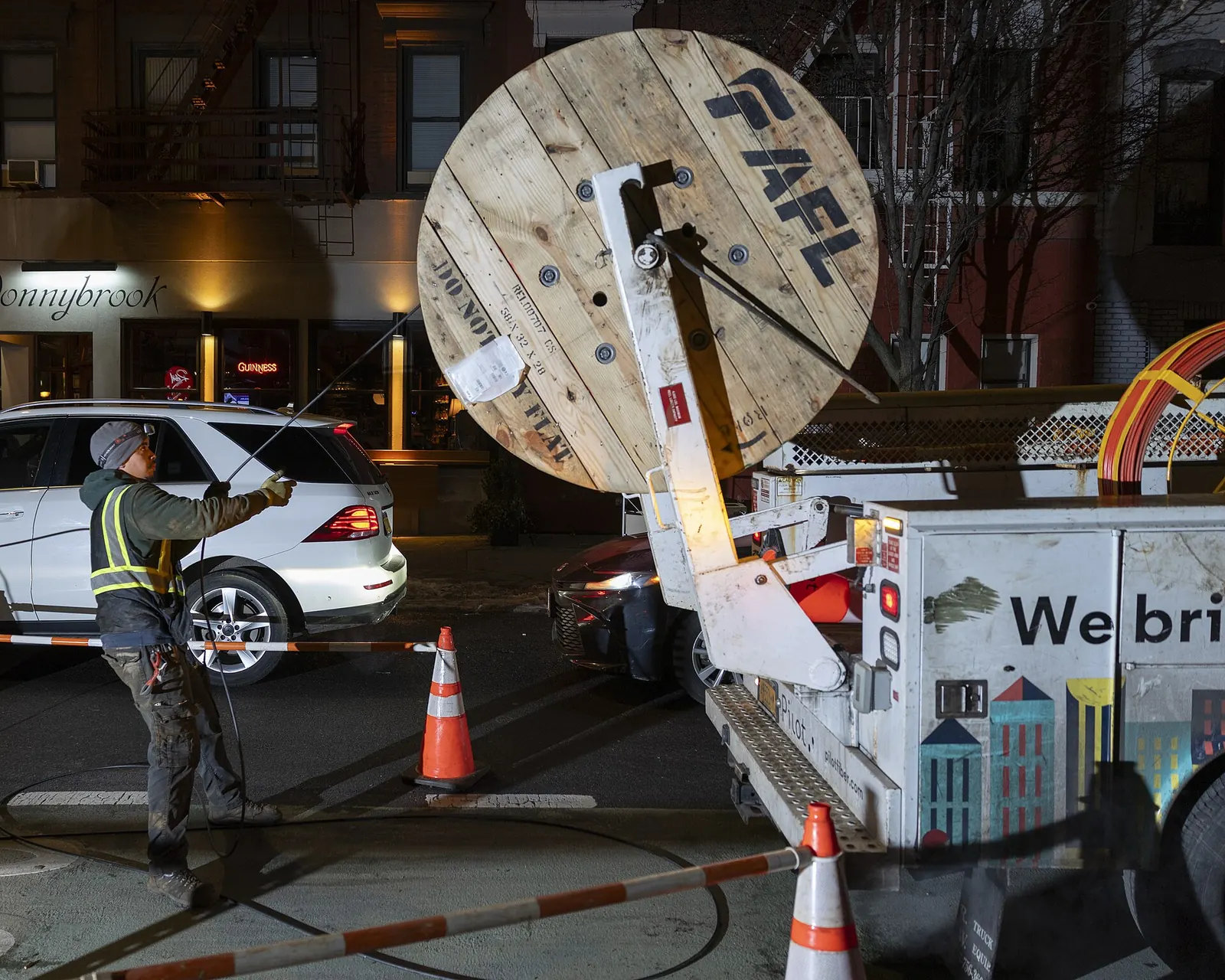
What makes Corning unusual is that it sells the passive part of the network (the glass, the cables, the connectors and the pre-terminated assemblies that let a contractor wire a data hall in days) rather than the active optics that turn electricity into light. That's a less glamorous business, but it doesn't become obsolete every two years. Prysmian, the Italian cable maker, is the other big winner. It signed a 10-year deal worth up to €5.5 billion in July 2026 to supply data-centre optical cable, and it's working with Relativity Networks on hollow-core fibre, in which light travels through air instead of glass and arrives nearly 50% sooner.
Layer 3: design
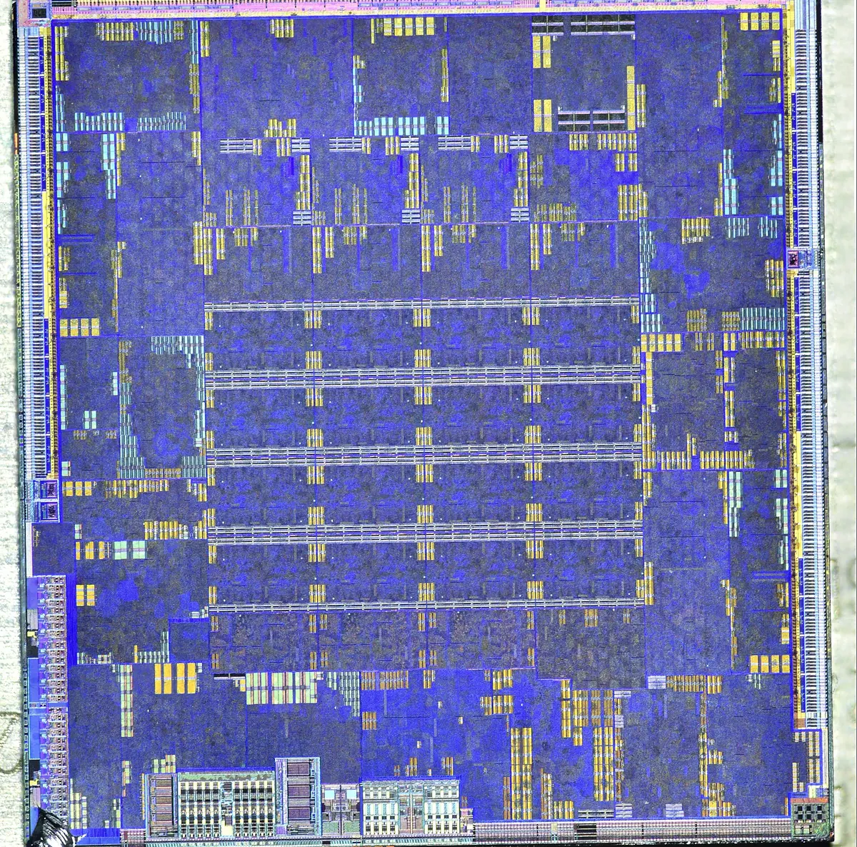
A modern accelerator has more than a hundred billion transistors. Nobody draws them by hand. They're described in code, synthesised into logic, placed, routed, simulated and verified with electronic design automation (EDA) software, and it's a near-duopoly.
Synopsys and Cadence each hold about 30% of the EDA market, with Siemens EDA (the former Mentor Graphics) at about 13%, according to TrendForce. Synopsys closed its acquisition of Ansys in July 2025, adding the physics simulation (heat, stress, electromagnetics) that matters more as chips get stacked in three dimensions. Cadence's edge is its hardware emulators, the room-sized machines that run a chip design before it exists so the software can be tested months before silicon. NVIDIA took a $2 billion stake in Synopsys in December 2025 to push GPU acceleration into the design flow. The cost of all this is high: IBS estimates that designing a large chip from scratch at 2 nm costs about $725 million, of which more than $300 million is software.
Then there's Arm. It doesn't make CPUs in the traditional sense (or didn't until this year). It licenses the instruction set and core designs that other companies build on. NVIDIA's Grace CPU uses Arm Neoverse cores. So do Amazon's Graviton, Microsoft's Cobalt and Google's Axion. In the quarter to June 2026, Arm's data-centre royalties more than doubled year on year. In March 2026 Arm crossed a line it had avoided for 35 years and launched a chip of its own, the AGI CPU, built on TSMC's 3 nm process with up to 136 cores and Meta as its lead customer. It now competes with some of its own licensees.
The third kind of designer is the custom-chip partner. Google, Amazon, Meta, Microsoft and OpenAI all design their own accelerators, but none of them does the whole job alone. Broadcom is the dominant partner: Google's TPU, Meta's MTIA and OpenAI's first chip, unveiled in June 2026, all run through it, and it counts six custom-accelerator customers. Marvell does the same for Amazon and Microsoft, and Alchip and GUC in Taiwan handle the physical back-end for others. Alchip's biggest customer (widely understood to be AWS) accounted for 60% of its 2024 revenue.
Layer 4: the tools
A chip fab is a building full of machines, and the machines are where the most extreme engineering in the chain lives.
ASML and the light that isn't light
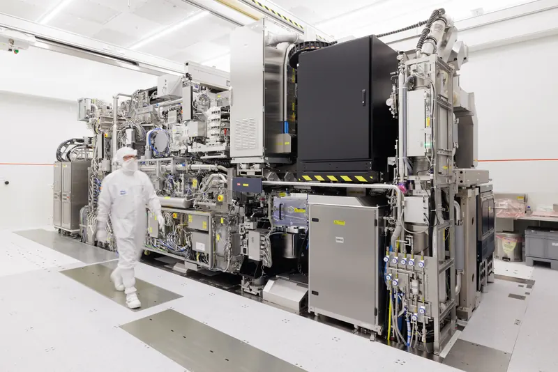
Leading-edge chips are printed with extreme ultraviolet (EUV) light at a wavelength of 13.5 nanometres. No lamp produces it and no lens can focus it. So ASML's machines make it: a droplet generator fires 50,000 drops of molten tin a second, a laser built by Trumpf hits each droplet twice, and the second pulse heats it to around 220,000°C, hotter than the surface of the sun, turning it into a plasma that glows at 13.5 nm. The light is gathered by mirrors from Zeiss that are so smooth that, scaled up to the size of Germany, the largest bump would be a tenth of a millimetre tall. The whole system sits in a vacuum because air would absorb the light.
ASML is the only company in the world that makes EUV scanners. A standard EUV machine costs well over $150 million; the new High-NA version, which prints finer lines, is estimated at about $380 million. ASML expects to ship about 65 standard EUV systems in 2026 and guides revenue at €43–45 billion. Intel shipped the first high-volume product made with High-NA in 2026. And because of export controls, China, which bought nearly half of ASML's machines in 2024, is guided at about 20% of 2026 sales.
Everyone else in the fab
Printing is one step of several hundred. A leading-edge wafer passes through 500 to more than 1,000 process steps and about 90 mask layers, and it spends three to four months in the fab. The other steps belong to a handful of companies:
| Company | What it does | Why it's hard to replace |
|---|---|---|
| Applied Materials | Deposition, etch, implant, polishing | The broadest toolset in the industry. It also owns about 9% of BESI, the hybrid-bonding leader. Record $9.1 billion quarter in July 2026 |
| Lam Research | Etch and deposition | The leader in the deep, narrow etches that 3D NAND and HBM depend on |
| Tokyo Electron | Coater/developers, etch, deposition | Close to 100% of the coater/developers that sit beside every EUV scanner (estimate) |
| KLA | Inspection and measurement | Over 85% of optical wafer inspection (estimate). Fabs can't find defects without it |
| Advantest | Chip testing | 66% of the testers for logic chips like GPUs, by its own estimate. Every AI chip gets tested before it's packaged |
| Disco | Dicing and grinding | Most of the world's dicing saws and grinders. Grinding is what makes HBM dies thin enough to stack |
SEMI counts $135 billion of equipment sold in 2025, with China the largest buyer at $49 billion, and it forecasts wafer fab equipment at $144 billion in 2026, up 23%.
Layer 5: the fabs
TSMC makes almost every AI accelerator in the world: NVIDIA's, AMD's, Google's TPU, Amazon's Trainium, Microsoft's Maia, Broadcom's custom parts, Cerebras's wafers. It had 72.5% of all foundry revenue in the second quarter of 2026, according to TrendForce. For leading-edge AI chips its share is effectively all of it, though no one publishes that number.
The results show what that position is worth. In the second quarter of 2026 TSMC's revenue rose 34% to $40.2 billion at a 67.7% gross margin, and high-performance computing was 66% of the total. Its 2 nm process (N2) reached revenue that quarter and should reach about 100,000 wafers a month by the end of 2026, by analyst estimates. A 2 nm wafer is priced at around $30,000. It raised 2026 capital spending to $60–64 billion. In August 2026 its monthly revenue hit a record NT$515 billion, up 53% year on year.
What makes TSMC unique isn't only its process technology. It's that it has spent forty years as a pure foundry that never competes with its customers, so every chip designer trusts it with its designs, and each generation's revenue funds the next. A leading-edge fab now costs roughly $28 billion (IBS estimate). Few companies can raise that; fewer still can fill it.
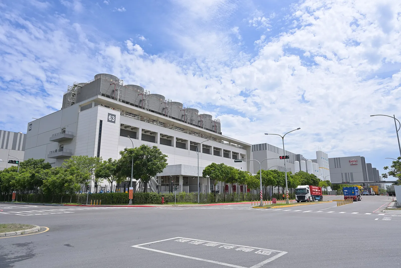
The alternatives are real but small. Samsung Foundry has 5.9% of the market. Its biggest AI win is a $16.5 billion contract with Tesla, running to 2033, to make Tesla's AI6 chip in Taylor, Texas. Intel is the only American company manufacturing leading-edge logic. Its 18A process is in volume production, 14A is due for risk production in 2027, and in 2025 it took in $8.9 billion from the US government (for 9.9%), $5 billion from NVIDIA and $2 billion from SoftBank. It still makes little money from outside customers ($293 million of external foundry revenue in the second quarter of 2026), but it has two things TSMC doesn't: it's American, and its x86 Xeon chips sit inside NVIDIA's own systems as the host processor. It also sells its EMIB packaging to other chipmakers as an alternative to TSMC's. Japan's Rapidus is trying to reach 2 nm in 2027, but it hasn't signed a volume customer yet.
Layer 6: packaging and memory
This is the leg of the journey that caught the industry out.
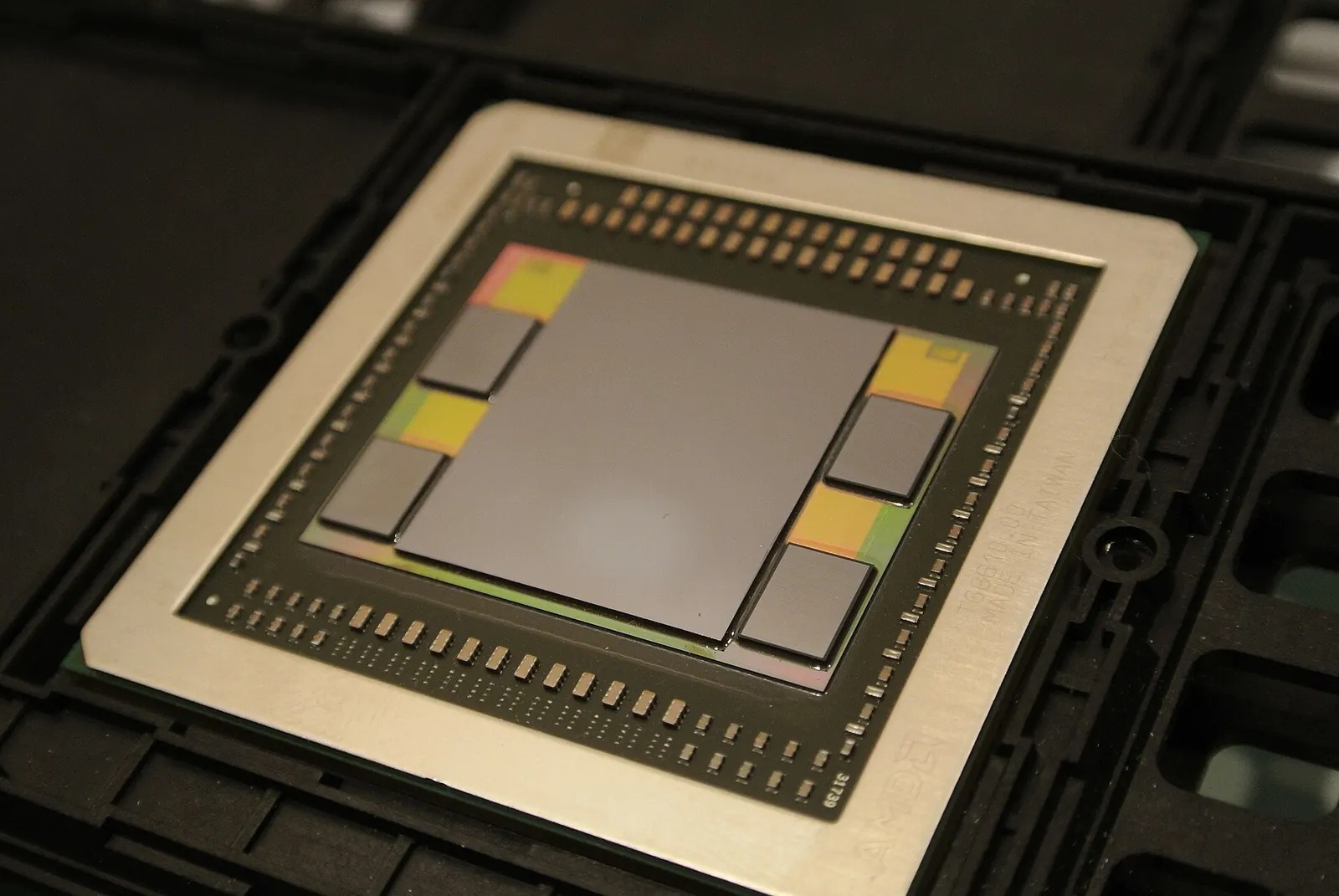
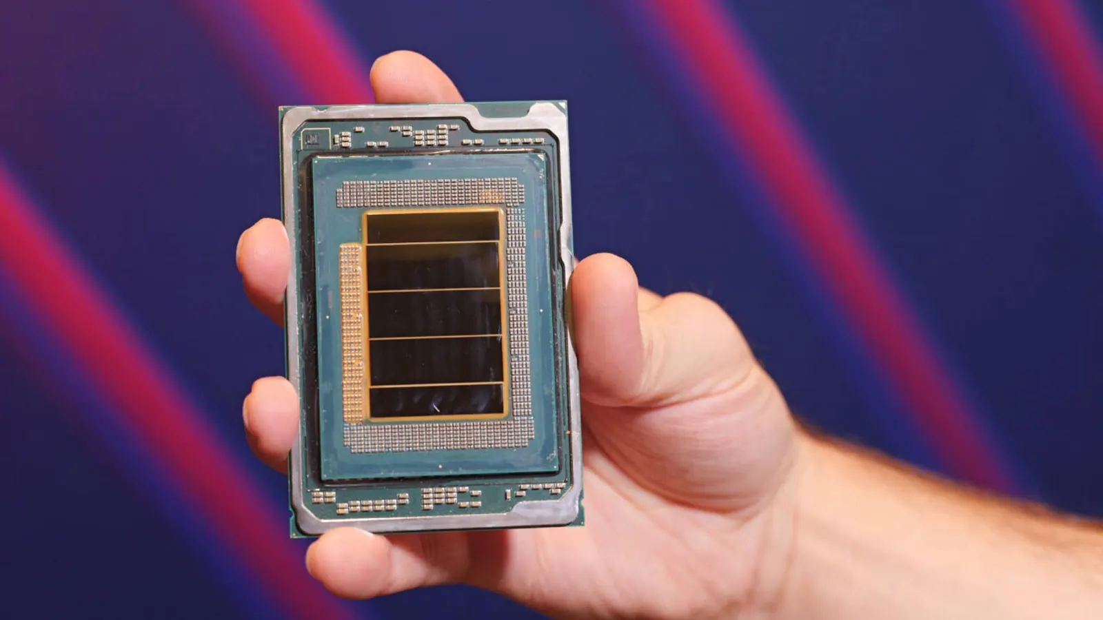
An AI accelerator isn't one chip. It's a system of chips assembled in a package: compute dies in the middle, stacks of high-bandwidth memory around them, all sitting on an interposer that wires them together with thousands of connections per square millimetre. TSMC's version is called CoWoS, short for Chip-on-Wafer-on-Substrate. Before 2023 it was a niche product for a few supercomputers. Then every AI chip needed it at once.
TSMC's CoWoS capacity has gone from roughly 30–40 thousand wafers a month at the end of 2024 to about 70–80 thousand at the end of 2025, and it's heading towards 120–140 thousand by the end of 2026, by TrendForce and other analyst estimates. It still hasn't caught up: the shortfall is estimated at 20% narrowing to 10% by year-end, and NVIDIA has booked about 60% of TSMC's CoWoS capacity for 2026–27. TSMC said on its July call that packaging remains "extremely tight". The overflow goes to outsourced assemblers. ASE raised its 2026 capex to a record $10.5 billion and expects its leading-edge packaging revenue to more than double this year. Amkor is building a $7 billion packaging campus in Arizona.
High-bandwidth memory
Each tower in that picture is an HBM stack: twelve DRAM dies, each ground thinner than a hair, stacked and wired through thousands of vertical holes called through-silicon vias. The point is width. A normal memory chip talks over a narrow bus; an HBM4 stack talks over a 2,048-bit interface sitting a few millimetres from the processor. An NVIDIA Rubin GPU carries eight stacks, 288 GB, at 22 terabytes per second.
HBM exists because of a problem that has been getting worse for a decade. The arithmetic a GPU can do has grown much faster than the rate at which memory can feed it.
Only three companies make HBM.
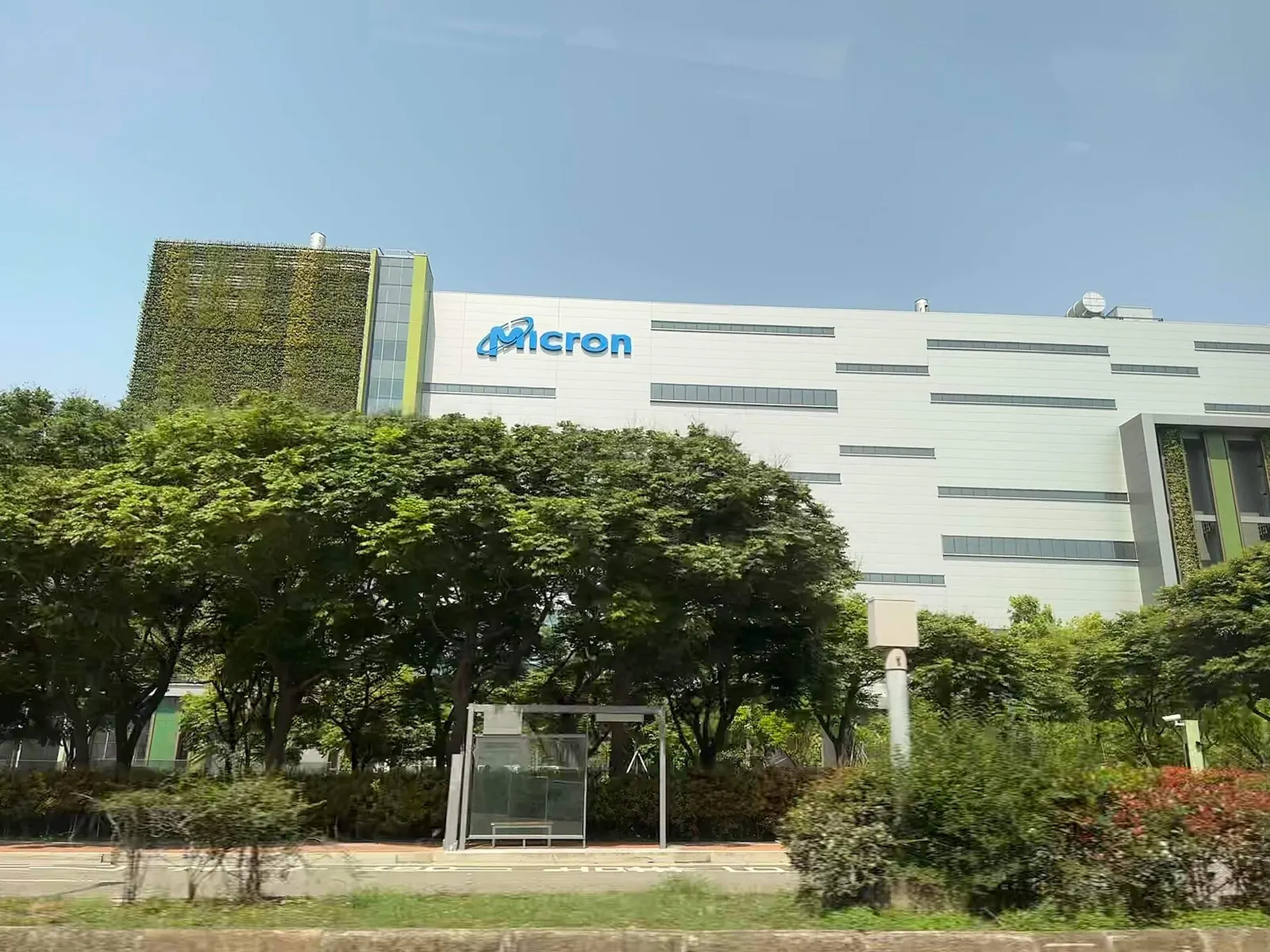
SK hynix bet on HBM early, when it was a niche product for graphics cards, and it's NVIDIA's lead supplier. In the second quarter of 2026 it made an operating profit of 60.5 trillion won on 79.3 trillion won of revenue, a 76% margin. Samsung, which had trouble qualifying its HBM3E with NVIDIA, started mass production of HBM4 in February 2026 and has doubled its share in a year. Micron is the only US maker. In its quarter to May 2026 its revenue was $41.5 billion, against $9.3 billion a year earlier, at an 84.6% gross margin. In December 2025 it shut its 29-year-old Crucial consumer brand to put every wafer into data-centre products.
The stacking itself is its own sub-industry. Korea's Hanmi Semiconductor has about 71% of the thermocompression bonders used to stack HBM, per TechInsights. From HBM4E onwards the industry expects to move to hybrid bonding, which joins copper directly to copper without solder bumps, and that's BESI's speciality: its orders more than doubled in the second quarter of 2026 and it now has 21 hybrid-bonding customers.
The memory boom spreads to flash
Because HBM uses about three times the wafer area of ordinary DRAM for the same capacity, every HBM stack takes supply away from the DRAM that goes into servers and PCs. The result in 2025–26 was the steepest memory price surge in the industry's history. TrendForce estimates that conventional DRAM contract prices rose 93–98% in a single quarter, the first of 2026.
Flash memory followed, for a different reason. When a model serves a long conversation, it keeps a cache of the attention state for every token so far (the KV cache, which comes up again in the inference section). That cache grows with context length and can reach tens of gigabytes per user. It doesn't fit in HBM, so it spills to CPU memory and then to SSDs. NVIDIA introduced a storage tier for exactly this in January 2026, built on its BlueField-4 processors and racks of flash drives.
SanDisk, spun out of Western Digital in February 2025 as a pure flash company, is the clearest example of what that did. Its data-centre revenue rose 437% in its latest quarter, its fiscal-year revenue rose 175% to $20.3 billion, and its stock was the best performer in the S&P 500 in 2025. It's working with SK hynix on "high-bandwidth flash", which stacks NAND like HBM to give accelerators a large, slower memory tier. The first samples are due in the second half of 2026. Kioxia and Seagate (hard drives, which still hold most of the world's AI training data) are riding the same wave.
Layer 7: the chips
NVIDIA
NVIDIA is the centre of the chain, and the numbers show it. In the quarter to July 2026 its revenue was $96.2 billion, up 106% year on year, with a 75% gross margin. Data centre was $89 billion of that, and it guided $108 billion for the next quarter. Management said growth next year would be about 70%, limited by supply, and that unconstrained demand would be about double. On the call, the finance chief said NVIDIA could capture about $40 billion of revenue in each gigawatt of data centre built with its new Vera Rubin chips.
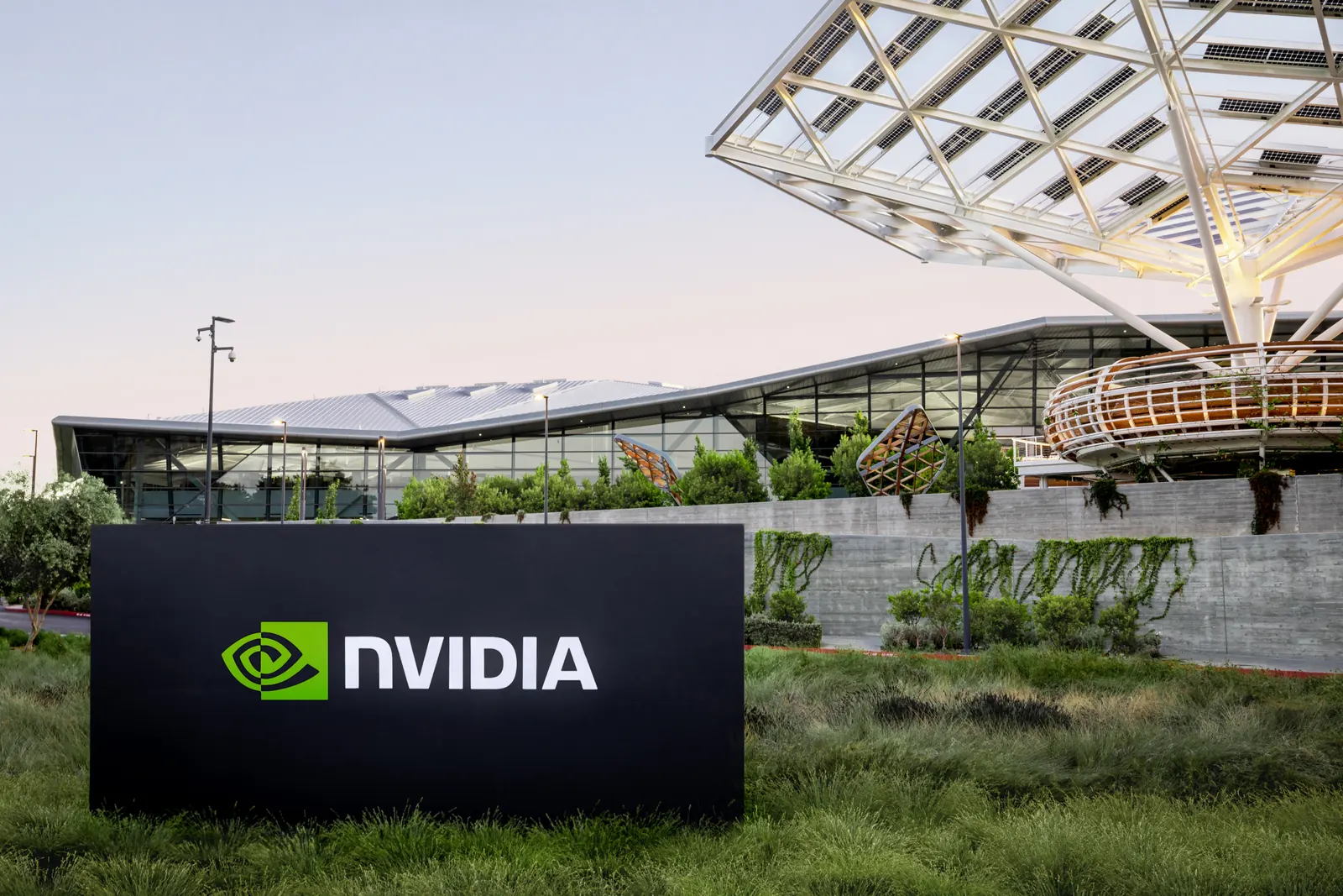
What makes NVIDIA unique isn't only the GPU. It sells the whole rack as one product: GPU, CPU (Grace, and now Vera), the NVLink switches that tie 72 GPUs into one, the network cards, the data processors, the Ethernet and InfiniBand switches and, underneath it all, CUDA, the software platform with about six million developers and twenty years of libraries. A competitor can match a chip. Matching the whole system, and the software people already wrote for it, is much harder.
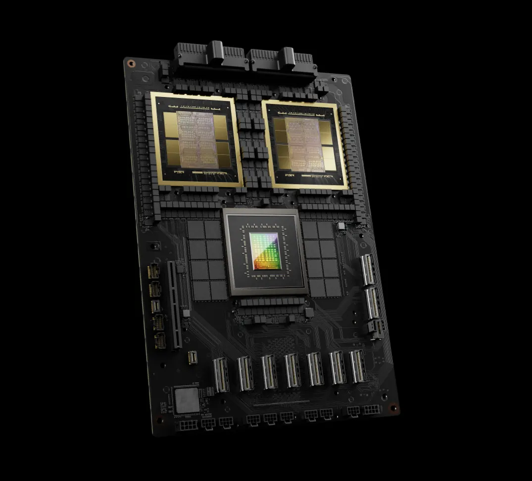
The current generation is Blackwell. A B200 GPU has 208 billion transistors across two dies and 192 GB of HBM3E at 8 TB/s; the Blackwell Ultra version carries 288 GB. The next generation, Vera Rubin, went into full production in August 2026. It pairs Rubin GPUs (288 GB of HBM4, 22 TB/s, 50 petaflops of 4-bit inference each) with Vera CPUs of 88 custom Arm cores, and management expects Rubin to make up about a fifth of data-centre revenue in its first full quarter. After that come Rubin Ultra in 2027, in "Kyber" racks drawing about 600 kW each, and Feynman in 2028.
NVIDIA has also been buying its way into the rest of the chain. In December 2025 it paid about $20 billion for a licence to Groq's inference chip technology and hired Groq's leadership; Groq-derived "LPX" racks are now in production. It invested $5 billion in Intel, $2 billion in Synopsys, up to $10 billion in Anthropic, and about $30 billion in OpenAI's 2026 funding round.
The alternatives
- AMD is the only company besides NVIDIA selling a rack-scale GPU system on the open market, and the only one with a leading server CPU as well. Its MI455X carries 432 GB of HBM4, more memory per GPU than NVIDIA's. Its "Helios" rack puts 72 of them together. OpenAI signed for 6 gigawatts over several generations in October 2025, receiving warrants for up to 10% of AMD, and Anthropic has signed for up to 2 GW. AMD's data-centre revenue more than doubled to $6.7 billion in the second quarter of 2026.
- Google's TPU is the most mature alternative. Ironwood, the seventh generation, links 9,216 chips in one pod. Google now rents TPUs outside its own cloud: Anthropic agreed in October 2025 to use up to a million of them, and Meta is renting TPUs and in talks to buy them for its own buildings. Broadcom co-designs them. Its AI chip revenue was $16.7 billion last quarter, up 221%.
- Amazon's Trainium, designed by its Annapurna Labs, powers Project Rainier, a cluster of about 500,000 Trainium2 chips built for Anthropic. Trainium3, on 3 nm, is now generally available.
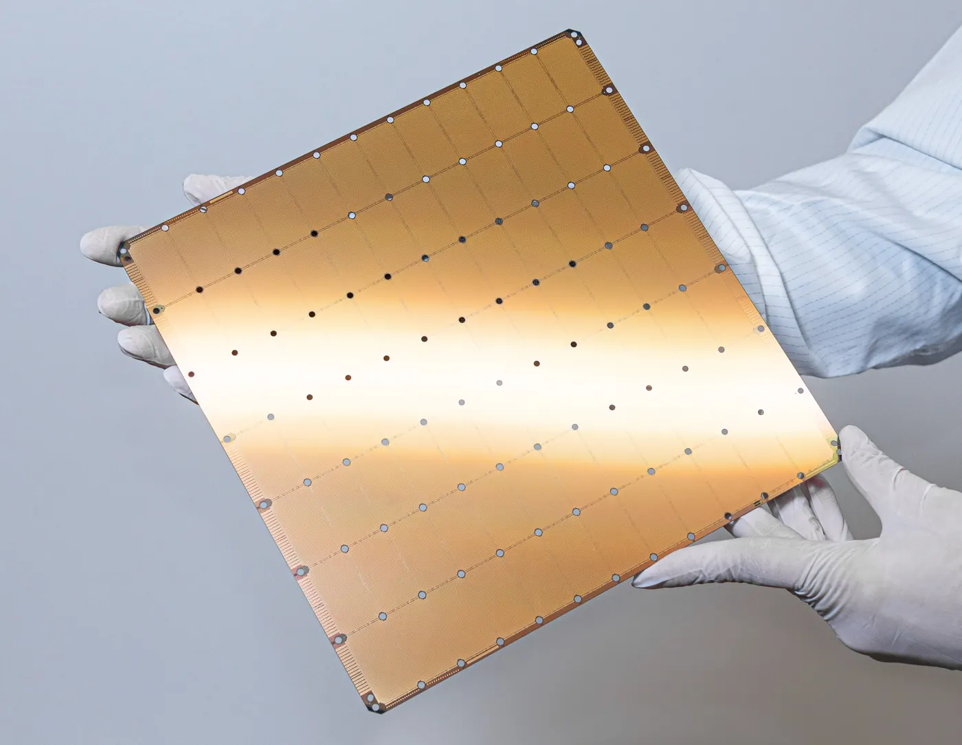
- Cerebras makes the only chip that is an entire wafer: 46,225 square millimetres, 4 trillion transistors and 44 GB of memory on the chip itself. Keeping the model's weights in on-chip memory lets it generate tokens very fast. OpenAI signed a deal worth more than $10 billion for 750 megawatts of Cerebras capacity in January 2026. Cerebras went public in May 2026, raising $5.55 billion, and its shares opened at more than double the offer price. Its main risk is concentration: two related customers in the UAE made up 86% of its 2025 revenue.
- Microsoft Maia 200, Meta MTIA, Etched (a chip that only runs transformers) and Tenstorrent (open RISC-V) complete the field.
CPUs matter again
For a few years the CPU in an AI server was an afterthought: one host processor to feed eight GPUs. Agents changed that. An agent spends much of its time running code, calling tools, searching and waiting, and all of that runs on CPUs. TrendForce says the CPU-to-GPU ratio in AI clusters has moved from 1:8 to 1:4 and is heading towards 1:1. Arm estimates that an agentic data centre needs about four times as many CPU cores per gigawatt as a classic AI one. Intel and AMD both raised server CPU prices in 2026, and lead times for some parts stretched past 30 weeks. Intel's data-centre revenue rose 59% last quarter. The x86 incumbent turns out to be an AI company after all.
Layer 8: systems
Chips become servers, and servers become racks. The unit of AI computing is now the rack, not the server.
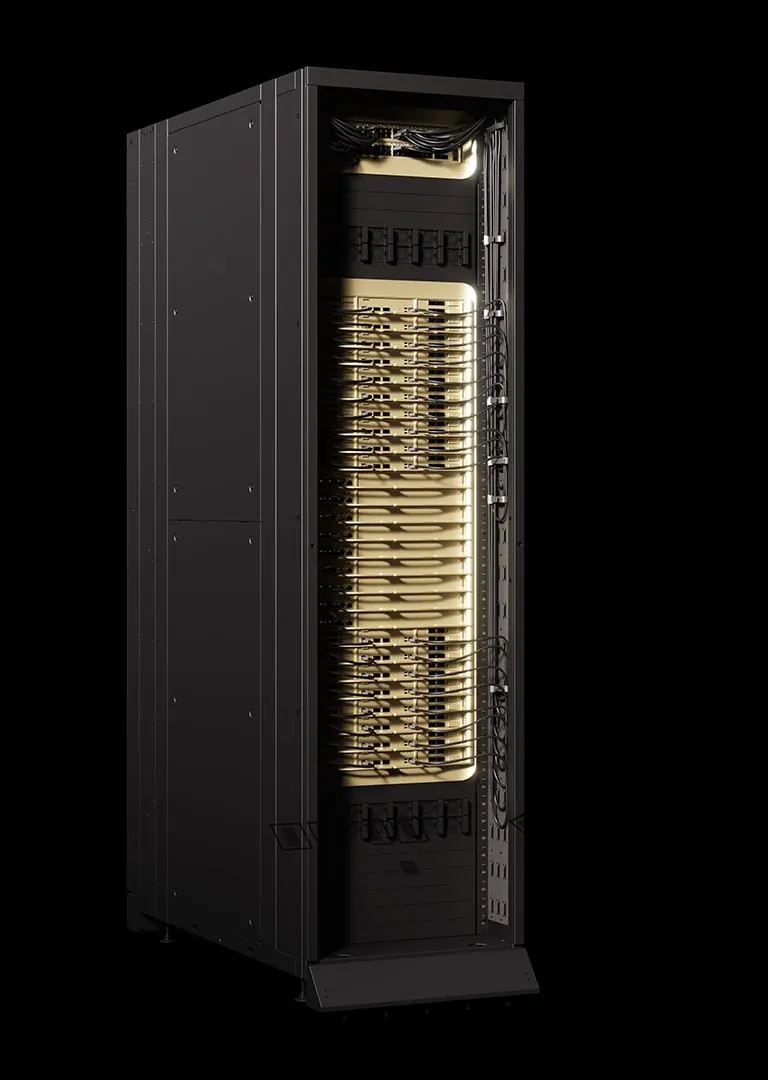
NVIDIA's GB300 NVL72 packs 72 GPUs and 36 CPUs into one liquid-cooled rack drawing about 135 kW and weighing about a tonne and a half. The 72 GPUs are joined by nine NVLink switch trays through a spine of about 5,000 copper cables, two miles of them, into what behaves like a single enormous GPU with 20 TB of HBM.
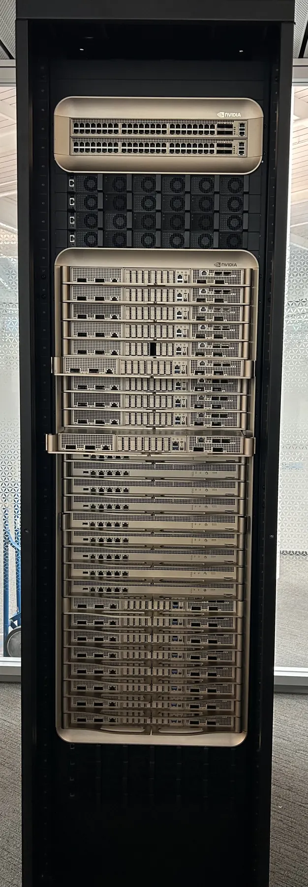
Racks like this are mostly assembled in Taiwan and Mexico by original design manufacturers. Foxconn is the largest: AI servers passed half of its revenue for the first time in the second quarter of 2026. Quanta, Wistron and Wiwynn are the others. The branded server makers sell the racks, finance them, install them and support them.
Dell has become the largest branded AI rack builder, selling to neoclouds, sovereign projects and enterprises. In the quarter to July 2026 it booked $60.9 billion of AI server orders, and its AI backlog rose from $51 billion to $95 billion in three months. It raised its full-year AI server revenue forecast to $74 billion and named memory, flash, CPUs and hard drives as its constraints. Supermicro, HPE and Lenovo are growing fast too, but at much thinner margins: Supermicro's gross margin was 17.5%. The server business adds value mainly through integration, speed and financing, and the market prices it that way.
The small parts that matter
Inside every rack are components worth a few dollars or a few hundred that the rack can't run without. Two of the most interesting belong to companies most people have never heard of.
SiTime makes timing chips: the oscillators and clock generators that give every other chip its heartbeat. A serial link running at 200 gigabits per second per lane has to sample its signal at exactly the right instant, trillions of times a second, and an optical module or network card has to stay synchronised with the one at the other end. SiTime's difference is that its resonators are microscopic silicon structures (MEMS) instead of the quartz crystals that have kept time in electronics for a century. They're smaller, more resistant to vibration and heat, and made in ordinary chip fabs. That used to be a niche. Now AI is its biggest market: SiTime's revenue rose 127% to $157 million in the second quarter of 2026, its communications, enterprise and data-centre segment rose 181%, and in July it closed a $1.5 billion purchase of Renesas's timing business.
Vicor solves a different physical problem. It's covered in the power section below, because it only makes sense once you see how many amps a GPU draws.
Layer 9: the network
AI training is a team sport played by tens of thousands of chips, and they spend a surprising share of their time waiting for each other. So the network that connects them matters almost as much as the chips. It comes in three scales. Scale-up makes a group of GPUs act like one (NVLink inside a rack). Scale-out connects racks within a building over InfiniBand or Ethernet. Scale-across connects buildings and campuses into one cluster. At each distance the right medium is different.
Copper, stretched
Copper wins over short distances because it doesn't need converting: an electrical signal goes in and an electrical signal comes out. The problem is that at 200 gigabits per second per lane, a signal on a passive copper cable degrades within a couple of metres.
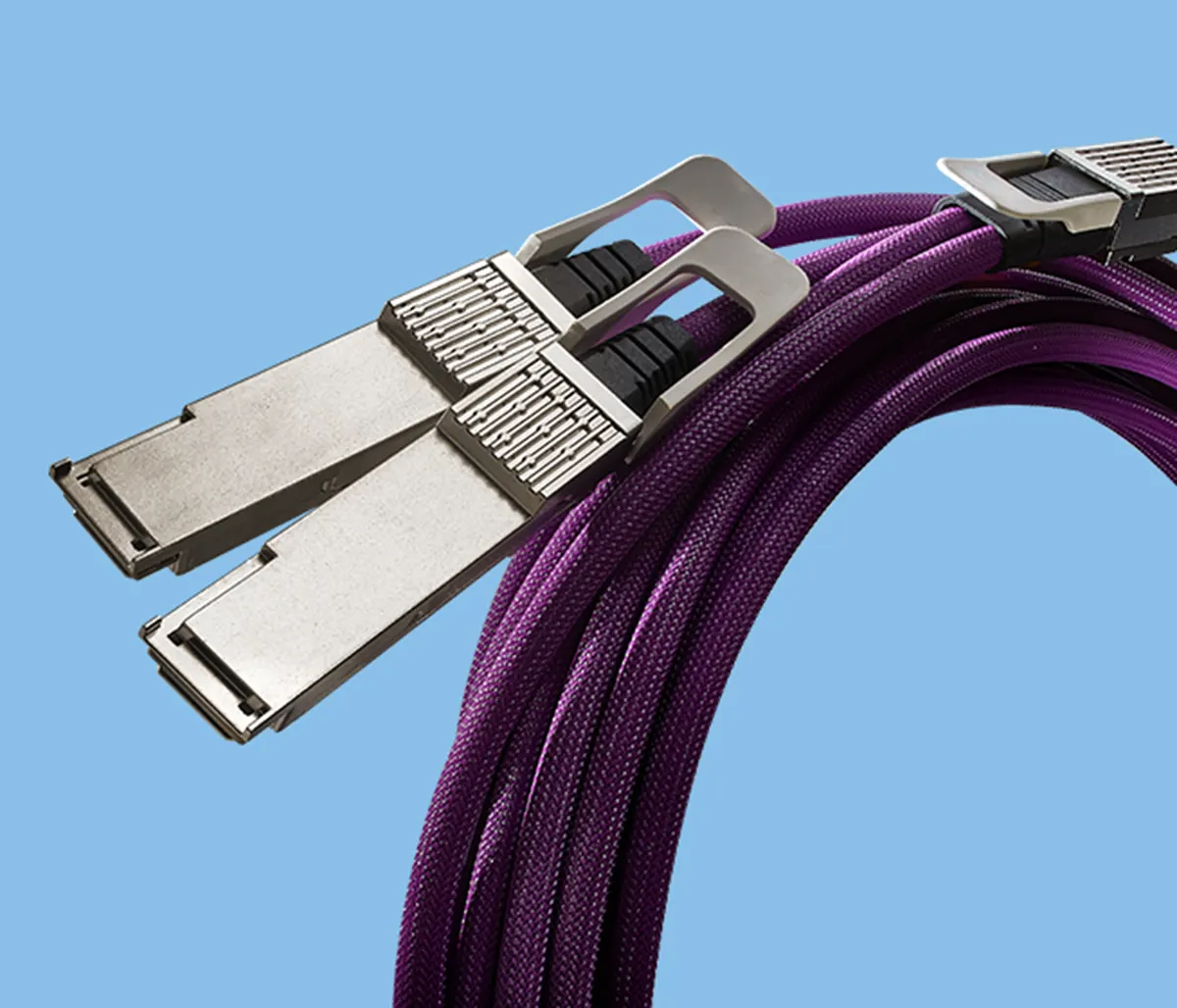
Credo found a middle way: the active electrical cable, or AEC. It's a copper cable with a small chip in each connector that cleans and retimes the signal, stretching copper's reach to about seven metres. That's enough to connect servers to the switch at the top of a rack, or neighbouring racks to each other. Credo says an AEC uses up to 14 watts less per link than the optical alternative and costs less, and, Credo argues, just as important in a cluster of 100,000 GPUs, it fails less often, because it has no lasers to degrade. Its purple cables are visible in AWS, Microsoft, xAI and Meta racks. In the quarter to July 2026 Credo's revenue grew 115% to $479 million, its seventh straight quarter of triple-digit growth. Its edge is that it designs its own ultra-low-power SerDes (the circuits that send and receive high-speed signals) and sells finished cables and optical modules with diagnostics software, not just chips. It's now pushing into optics too.
Astera Labs makes the retimers that stretch PCIe signals across a circuit board, and now switch chips for scale-up networks. Its revenue doubled year on year last quarter and it's guiding for another 40% jump this quarter. Marvell supplies the digital signal processors inside most high-speed optical modules and, with its $3.25 billion purchase of Celestial AI, is betting that light will eventually reach inside the rack too.
Light
Beyond a few metres, the signal becomes light. An optical transceiver, a module about the size of a pack of gum, converts electrical signals to laser pulses and back. An NVIDIA cluster uses roughly one 800-gigabit transceiver per GPU on its back-end network alone. The lasers inside are made of indium phosphide, and they became one of 2026's bottlenecks.
- Coherent is the most vertically integrated: it makes indium phosphide wafers, lasers and finished transceivers, and it built the world's first six-inch indium phosphide fabs, in Texas and Sweden, which cut the cost per laser by about 60%. Its data-centre and communications revenue rose 59% last quarter.
- Lumentum makes the lasers inside other companies' modules, plus optical circuit switches: mirrors that physically redirect light between fibres, which Google pioneered in its TPU clusters. Its revenue doubled last quarter to just over $1 billion, and it's reported to be sold out into 2028.
- Innolight and Eoptolink in China build most of the world's 800-gigabit and 1.6-terabit transceivers. Fabrinet in Thailand assembles optics for NVIDIA and Cisco.
- Switch silicon comes from Broadcom (Tomahawk 6, the first 102.4-terabit switch chip) and NVIDIA (Spectrum-X). The boxes come from Arista, whose revenue passed $3 billion a quarter, and Cisco, which took $9.3 billion of AI infrastructure orders from hyperscalers in its last fiscal year.
- NVIDIA's co-packaged optics (lasers mounted next to the switch chip instead of in pluggable modules) promise 3.5 times better power efficiency. Its first switches using them are shipping now.
Between buildings, the fibre carries coherent optics that encode data in the phase of light, the same technique long-haul telecom networks use. Ciena leads here, and cloud providers now make up more than half of its revenue. Across oceans, hyperscalers own or lease about three-quarters of all international bandwidth, and they build their own cables. Meta's Project Waterworth will run 50,000 km, longer than the Earth's circumference. The cables are laid by SubCom, ASN and NEC, which together build about 90% of the world's subsea systems.

Layer 10: the buildings
Power, from the grid to the transistor
This is the diagram that best explains why AI data centres are hard to build.
Electricity reaches a data centre at hundreds of thousands of volts and has to reach the GPU at less than one volt. Every step down in voltage is a step up in current, because power is volts times amps. At the end of the chain, a GPU drawing about 1.4 kW at 0.8 V needs roughly 1,750 amps. For comparison, a house in the US is usually wired for 200. And it has to be delivered to a chip a few centimetres across, through the board, without melting anything or losing half the energy as heat along the way.
Vicor's whole company is built on that last centimetre. Traditional voltage regulators sit beside the processor and push current sideways through the circuit board, which wastes power and takes up space. Vicor's "Factorized Power Architecture" splits the conversion into two stages, and its "vertical power delivery" puts the final stage directly underneath the processor, feeding current straight up into it. Its second generation reaches three amps per square millimetre. Vicor has also been an aggressive defender of its patents: after an International Trade Commission case, it has signed a licence that pays it $5 million a quarter in royalties this year and $10 million next year, and a second case targeting unlicensed converters is due for a final decision in 2027. It's a small company, about $600 million of expected 2026 revenue with a one-year backlog up 145%, holding an unusually specific piece of intellectual property. Monolithic Power Systems, Infineon and Renesas are its main competitors for the same job.
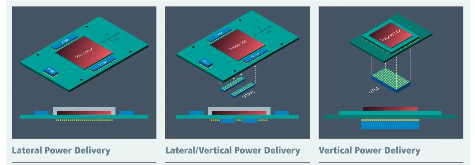
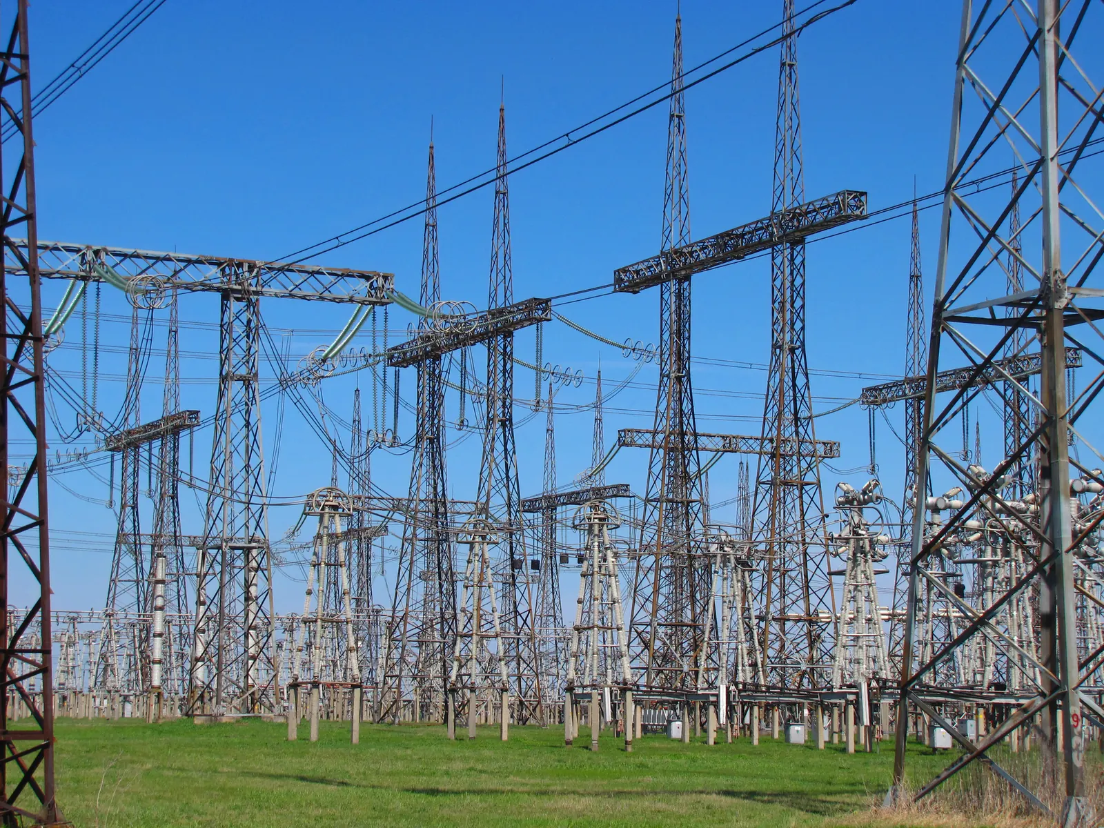
Higher up the staircase, the power equipment comes from Schneider Electric, Eaton, ABB and Vertiv (switchgear, uninterruptible power supplies, busways), and the rack power shelves mostly from Taiwan's Delta and Lite-On. The dashed line in the diagram is the next big change. For its 2027 Kyber racks, which draw up to 600 kW each, NVIDIA is moving to 800-volt direct current delivered straight to the rack. That cuts copper by about 45% and removes several conversion steps. It depends on power switches made from silicon carbide and gallium nitride (Infineon, onsemi, STMicro, Navitas, Wolfspeed), materials that until now were known mainly from electric cars.
Heat
Almost every watt that goes into a chip comes out as heat. At 135 kW per rack, air can't carry it away fast enough, so the heat leaves in liquid: cold plates sit on every chip, fed by coolant distribution units that pump water through the rack and out to chillers or dry coolers. TrendForce estimates that 53% of AI chips shipped in 2026 will be liquid-cooled, up from 33% in 2025.
Vertiv is the company most closely tied to this shift. It sells both halves of the building's mechanical and electrical plant (power: UPS, switchgear, busway; thermal: CDUs, chillers, heat rejection) and it co-designs reference architectures with NVIDIA, so a customer building for the next generation of GPUs can buy a matched set. Its revenue grew 24% in the second quarter of 2026, but its organic orders rose 152%, which says more about where it's heading. Its competitors are consolidating to catch up: Eaton bought Boyd Thermal for $9.5 billion, and Schneider bought Motivair.
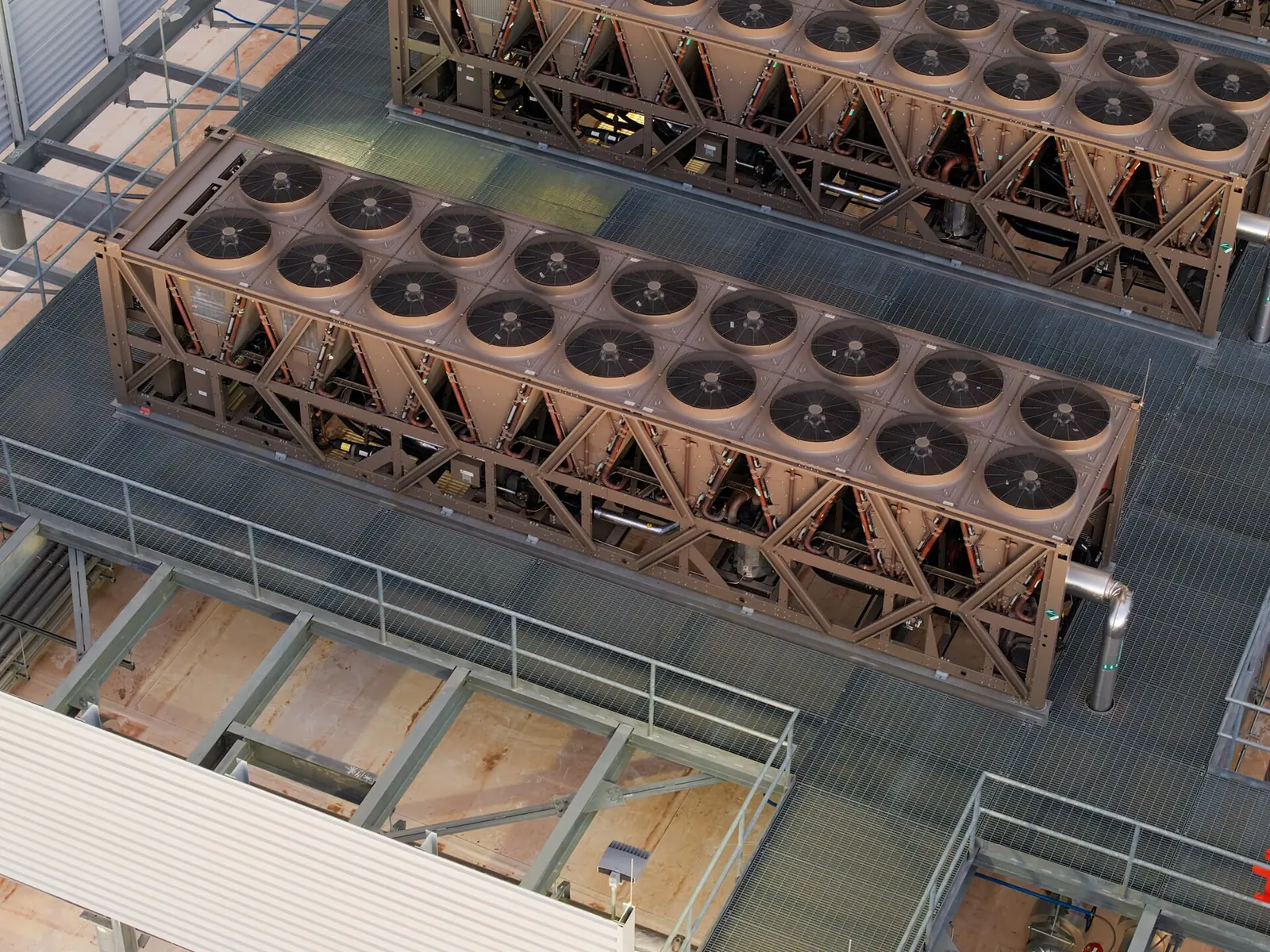
The best-run data centres are now remarkably efficient. Google's fleet runs at a power usage effectiveness of 1.09, meaning only 9% of energy goes to anything other than the computers, against an industry average of 1.54. Microsoft's Fairwater site in Wisconsin uses a closed-loop liquid system that needs water only when it's first filled.
Layer 11: energy
Data centres used about 415 terawatt-hours of electricity in 2024, about 1.5% of the world's supply, according to the International Energy Agency. Its base case more than doubles that to 945 TWh by 2030, with accelerated servers driving about half of the increase. In the US, Lawrence Berkeley National Laboratory estimates data centres went from 58 TWh in 2014 to 176 TWh in 2023, 4.4% of all electricity, and projects 6.7% to 12% by 2028.
In 2024 that electricity came from coal (30%), renewables (27%), gas (26%) and nuclear (15%). Coal's share is high because of China. In the US, gas supplies more than 40% of data-centre power and, with renewables, is expected to meet most of the increase through 2030. What's changed is that the biggest buyers no longer want to wait for the grid.
Gas turbines, sold out
The quickest way to add firm power is a gas turbine, and there are only three large makers: GE Vernova, Siemens Energy and Mitsubishi Power. GE Vernova's gas backlog and slot reservations reached 116 gigawatts in the second quarter of 2026. It's now taking reservations for 2031 and expects that year to be more than half booked by the end of 2026. Data centres make up about a fifth of its gas customers, and its data-centre orders in the first half of 2026 were more than double all of 2025. Some builders have gone further and put the turbines on site: xAI's Colossus 2 in Memphis has a permitted 1.2 GW gas plant of its own.
Bloom Energy: power without the grid or a flame
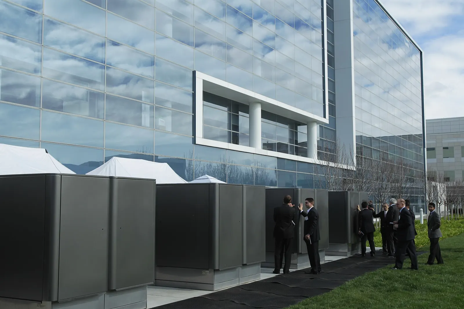
Bloom Energy makes solid-oxide fuel cells, which convert natural gas (or hydrogen) into electricity chemically, without combustion, in cabinets that can be installed in modular blocks. What it's really selling is speed. A data centre that can't get a grid connection for five years, or a turbine until 2030, can install Bloom's units in months, right next to the building, with much lower local emissions than burning the same gas. That pitch turned Bloom from a niche clean-energy company into AI infrastructure. American Electric Power signed a $2.65 billion deal for up to 1 GW in January 2026; Brookfield committed up to $5 billion in October 2025; Oracle, Equinix and "all the major US hyperscalers" have approved its systems. In the second quarter of 2026 its revenue rose 166% to more than $1 billion, and it guides to roughly double for the year.
Nuclear, later
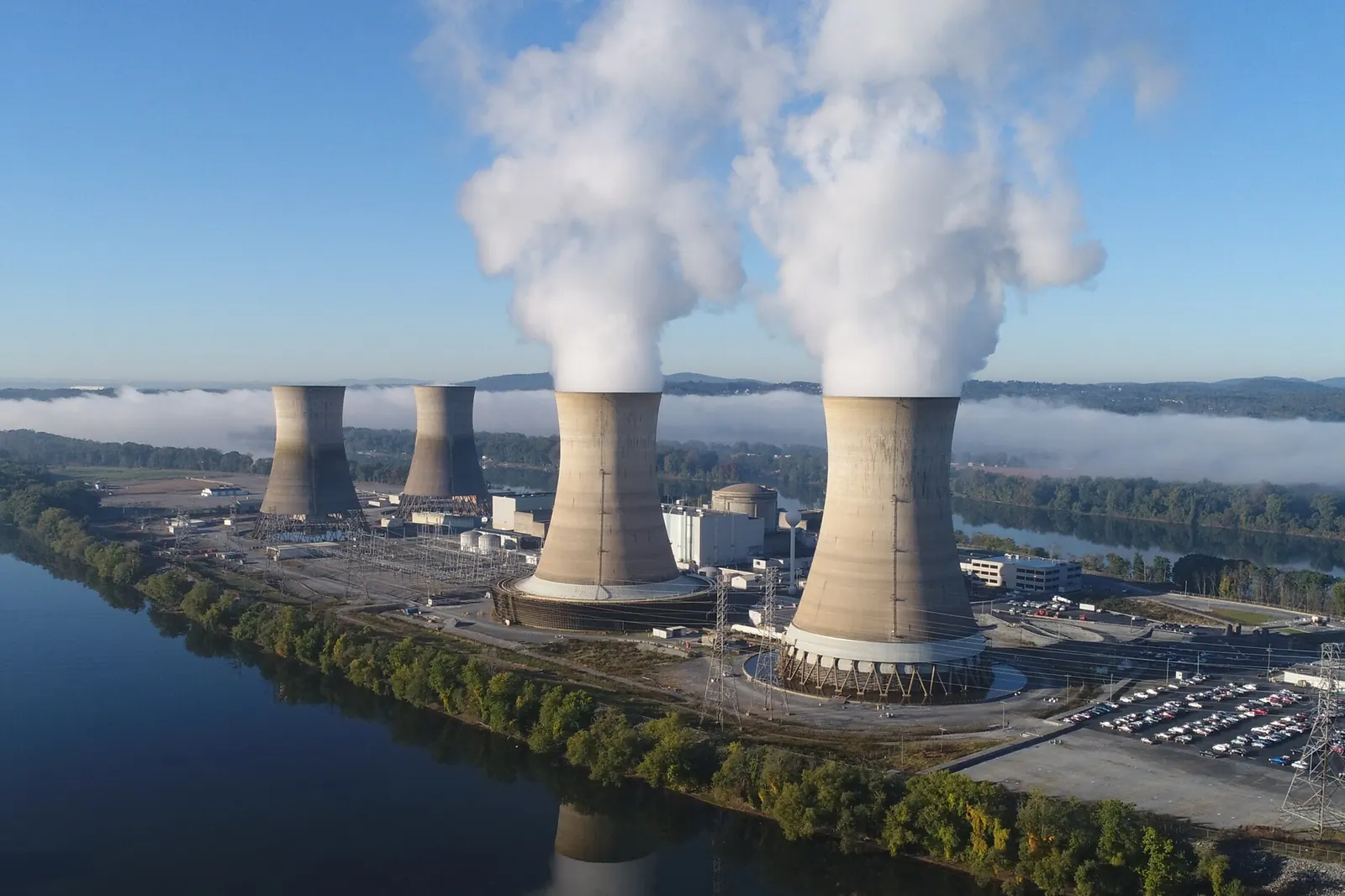
The nuclear deals are the most striking and the slowest. Microsoft is paying to restart Three Mile Island unit 1, now renamed the Crane Clean Energy Center, with Constellation, targeting 2027. Amazon buys 1.92 GW from Talen's Susquehanna plant. Meta signed deals in January 2026 for up to 6.6 GW by 2035 with Vistra (existing plants), TerraPower and Oklo (new reactors). Google backs Kairos Power and Amazon X-energy. Most of the new reactors arrive after 2030. For this decade, gas, solar plus batteries, and fuel cells carry the load.
The campuses and the money
Put all of this together and you get campuses measured in gigawatts. OpenAI, Oracle and SoftBank's Stargate had announced about 7 GW of sites by late 2025, starting with Abilene, Texas, built by Crusoe. Meta's Hyperion in Louisiana is planned for 5 GW. xAI built Colossus 1 in Memphis in 122 days. Microsoft's Fairwater in Wisconsin has 120 miles of medium-voltage cable. Anthropic committed $50 billion to its own data centres in Texas and New York with Fluidstack. Around them sit the neoclouds (CoreWeave, Nebius, Crusoe) and the colocation landlords (Equinix, Digital Realty) who rent space, power and increasingly GPUs.
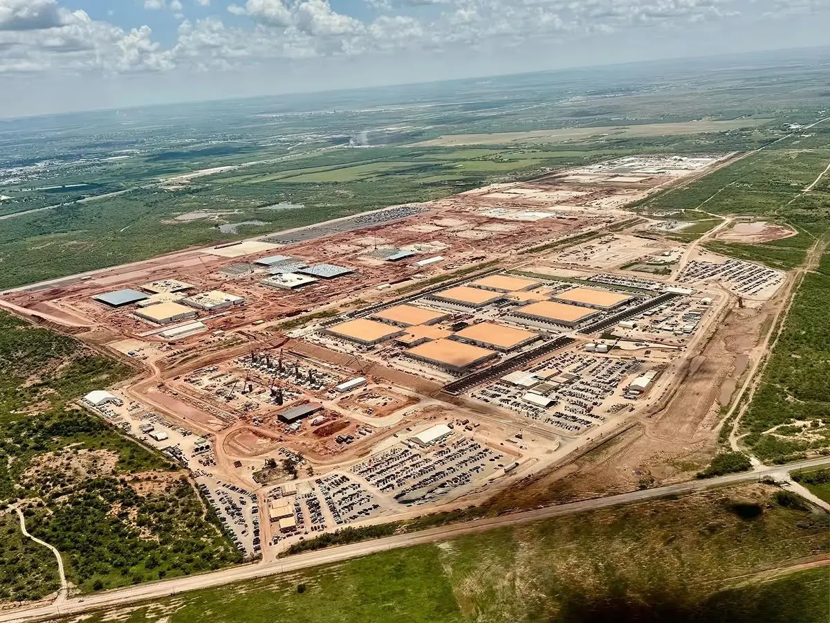
The spending is the largest private capital programme in history. Amazon plans about $220 billion of capital spending in 2026, Alphabet $195–205 billion, Meta $130–145 billion. Oracle expects $90–95 billion gross in its current fiscal year and has $664 billion of contracted future revenue. Amazon's CEO said the company would "still not have enough capacity" in 2026, and that the same would be true in 2027. NVIDIA puts the five largest hyperscalers at nearly $800 billion this year and $1.3 trillion next.
The per-gigawatt numbers show how the money is divided. NVIDIA says it can capture about $40 billion of a Rubin-generation gigawatt, and Huang put the all-in cost of a gigawatt at $50–60 billion a year earlier. Much of the chain upstream (TSMC's wafers, the HBM, the packaging, the substrates) is paid for inside NVIDIA's share, because NVIDIA buys those parts. What's left outside it, perhaps a quarter to a third of the total, pays for the power equipment, the cooling, other networking, the building, the land and the grid connection. That's a smaller slice per gigawatt, but it's paid on every gigawatt, whoever's chips go inside.
Layer 12: the models
Now the software, where the minerals finally become an LLM: how the people at AI labs turn all this hardware into a model.
Most compute goes into experiments
The first surprise is where the compute goes. The famous training run, the one that produces the released model, is the tip of a pyramid. Before it, researchers run hundreds or thousands of smaller experiments to decide the recipe: the architecture, the data mix, the learning rate schedule, how big to go. They fit those small runs to scaling laws and extrapolate to the big one.
Epoch AI estimates that in 2024 OpenAI spent about $5 billion on research compute, of which only about 10% went into the final training runs of models it released. At MiniMax and Zhipu (Z.ai), two Chinese labs, the share was 12–23%. Most of a lab's compute budget is spent learning how to train, not training.
The recipe
Data. A frontier model starts with tens of trillions of tokens (a token is roughly three-quarters of a word). Most of it is crawled from the web. Hugging Face's open FineWeb dataset, 15 trillion tokens built from 96 snapshots of Common Crawl, shows the process: extract the text, filter out spam and junk with rules and classifiers, remove near-duplicates (FineWeb's MinHash step compares five-word fragments), strip personal information and tokenise. Labs add licensed content, code, books, maths and increasingly synthetic data generated by earlier models. Meta's Llama 3 used about 15 trillion tokens, Alibaba's Qwen3 about 36 trillion and DeepSeek's V4 about 33 trillion. Data also has legal costs now: Anthropic agreed a $1.5 billion settlement in 2025 with authors whose books had been taken from pirate sites.
Pretraining. The model, a transformer and now usually a mixture-of-experts transformer in which only a fraction of the parameters is active for each token, learns to predict the next token, over and over, for months. DeepSeek-V3 had 671 billion parameters but used only 37 billion per token. Its final run took 2.8 million GPU-hours on 2,048 H800s, which DeepSeek priced at $5.6 million, excluding all the experiments before it. The largest runs are far bigger. Epoch estimates Grok 4 at about 5×10²⁶ floating-point operations, 246 million H100-hours and about $490 million. OpenAI's GPT-6 Astra, released this month, is the first it has pretrained on more than 100,000 GPUs, and Epoch's preliminary estimate is about 10²⁷ operations. Epoch says frontier training compute has grown about fivefold a year since 2020.
Parallelism. No GPU can hold a frontier model, let alone train one alone, so the work is split several ways at once.
The tools for this are mostly open source. PyTorch, from Meta, is the dominant framework, with FSDP to shard models across GPUs and TorchTitan to combine four kinds of parallelism. Google and some other labs use JAX, compiled by XLA onto TPUs; Anthropic has said it uses PyTorch, JAX and Triton, OpenAI's language for writing GPU kernels. NVIDIA's Megatron-Core and Microsoft's DeepSpeed provide the large-scale parallelism recipes many labs start from. Jobs are scheduled with Slurm or Kubernetes; experiments are tracked in tools like Weights & Biases, which CoreWeave bought for about $1.7 billion in 2025. Precision keeps falling to save memory and energy: most runs now train in 8-bit floating point, and NVIDIA has shown that 4-bit (NVFP4) can match it over a 10-trillion-token run.
At this scale, failure is routine. Meta's Llama 3 paper recorded 466 interruptions in 54 days on 16,384 H100s, about one every three hours. Of the unexpected ones, about 78% were traced to hardware, and HBM memory alone caused 17%. Checkpointing, automatic restarts and spare capacity are as much a part of training as the maths.
Post-training. A pretrained model is a superb autocomplete, not an assistant. Post-training turns it into one. It starts with supervised fine-tuning on examples written by experts, continues with learning from preferences (the RLHF that made ChatGPT possible in 2022, and variants like Anthropic's Constitutional AI and DPO), and now leans heavily on reinforcement learning against verifiable rewards: the model tries a maths problem or a coding task thousands of times, and the attempts that pass the tests are reinforced. That's how reasoning models were made, and it has become expensive. xAI said Grok 4 ran reinforcement learning "at pretraining scale".
That created a new supply chain of its own. Labs buy RL environments, simulated websites, apps and codebases where agents can practise tasks. Epoch reports that a replica of a simple website costs around $20,000 and a complex app like Slack around $300,000. They also buy expert data from companies like Scale AI (49% owned by Meta since June 2025), Surge AI, Mercor and Turing, which pay doctors, lawyers and engineers to write and grade examples. Mercor alone is reported to have passed a $2 billion revenue run-rate.
Evaluation and safety. Before release, models are tested against benchmarks, attacked by internal and external red teams, and checked for dangerous capabilities, then released in stages. It's the shortest step in calendar time and the one that decides whether everything above ships.
And increasingly, the models help build their successors. Anthropic reported that more than 80% of the code merged at the company in May 2026 was written by Claude, and that a typical engineer merged eight times more code per day than in 2024.
Layer 13: inference, or how the answer reaches you
Training happens once. Inference, running the model to answer requests, happens every time anyone uses it, and it's now the bigger business. Here's what happens when you press enter.
Your request travels to the nearest data centre with capacity, passes through an API gateway and a router that picks a model replica, and waits briefly in a queue. Then the work splits into two very different phases.
Prefill reads your whole prompt at once. Every token is processed in parallel, so the GPUs are busy doing arithmetic, and the result is the KV cache: the attention state for every token so far. Decode then generates the answer one token at a time. For each new token the GPU has to read the model's weights and the whole KV cache out of memory again, so decode is limited by memory bandwidth, not compute. That's why the HBM section mattered: a 70-billion-parameter model in 16-bit precision is about 140 GB, and an H100 reading it at 3.35 TB/s can produce at most about 24 tokens a second for a single user. The KV cache for that same model is about 320 KB per token, so a 128,000-token conversation needs about 40 GB of memory for one user.
Serving software exists to get around those limits:
- Batching serves many users at once, so the weights read from memory are reused across all of them. vLLM's PagedAttention, from Berkeley, manages KV-cache memory the way an operating system manages pages and raised throughput two to four times over earlier systems. vLLM, SGLang and NVIDIA's TensorRT-LLM are the main open-source serving engines.
- Disaggregation runs prefill and decode on different machines, each tuned for its phase, and ships the KV cache between them. NVIDIA's Dynamo does this and claims up to 30 times more requests served for DeepSeek-R1 on its Blackwell racks.
- Caching keeps the KV cache of common prompts (system instructions, long documents) so they aren't recomputed. Providers pass the saving on: cached input tokens cost a tenth or less of fresh ones.
- Smaller numbers and smaller models: quantisation to 8 or 4 bits, distillation of big models into small ones, speculative decoding (a small model drafts, the big one checks), and mixture-of-experts designs that activate a fraction of the weights per token.
Those techniques, together with better chips, have made intelligence dramatically cheaper. Andreessen Horowitz calculated that the price of a given level of capability fell about tenfold a year between 2021 and 2024. Epoch finds a median decline of about 50 times a year across benchmarks. GPT-4 cost $30 per million input tokens at launch in March 2023; GPT-5 launched at $1.25 in 2025, and today small models from OpenAI and DeepSeek cost a few cents.
Falling prices have been met by rising use.
Google processed 9.7 trillion tokens a month in 2024 and more than 3.2 quadrillion a month in May 2026. Its API alone was handling about 19 billion tokens a minute. Microsoft says the number of customers running at a trillion tokens a year has quadrupled. Much of the new traffic is agents, which read and write far more per task than a person chatting.
A new layer of companies has formed to serve it. Beyond the labs' own APIs and the big clouds, inference specialists like Fireworks (valued at $17.5 billion, with more than $1 billion of annualised revenue), Baseten and Together AI run open and custom models for developers, while Cerebras and NVIDIA's Groq-derived systems compete on raw speed. OpenRouter routes developer traffic across all of them; in one week this summer DeepSeek's V4 Flash processed 7.2 trillion tokens through it alone.
What the whole chain looks like from the top
Put the latest quarter's growth for each layer side by side, and a pattern appears.
The fastest growth is in whatever is scarcest: memory, accelerators, and the chips and cables that connect them. The slowest is in the heavy layers (fabs, tools, cooling, glass), but that's partly a timing effect: those companies book orders years before they recognise the revenue. Vertiv's orders rose six times faster than its sales. GE Vernova is booking turbines for 2031.
And the binding constraint keeps moving.
In 2023 it was CoWoS packaging. In 2024 it was HBM, then grid connections and transformers. In 2025 gas turbines sold out years ahead. By late 2025 the memory makers had run out of DRAM and flash, and in 2026 indium phosphide lasers and server CPUs joined the list. Foxconn's chairman already names advanced packaging as the ceiling for 2027. Each time the bottleneck moves, pricing power moves with it, to whichever company holds the scarce layer.
That's the most useful way I've found to read this industry. It's not one bet on "AI". It's a chain of very different businesses: a quartz mine, a chemical company, a lithography monopoly, a foundry, three memory makers, a cable maker, a timing company, a power-module specialist, a turbine maker, a fuel-cell company, a few labs and a lot of serving software. Each is tied to the same demand, but each has its own physics, its own competitors and its own timing. When someone tells you AI is a bubble or a revolution, the more useful question is which layer they mean, and whether that layer is the one running short right now.
So the next time a chatbot answers you in a second, remember the trip behind it: quartz and copper out of the ground, through thirteen industries and a few of the hardest machines ever built, into a model that turns it all back into words. That's the adventure. Every layer of it is a business, and every one of them is still being built.